This page is more of a blog about my work with IC CAD programs like Cadence Virtuoso and Magic VLSI because I don't entirely know what I'm doing, so I'm just shooting the shit. This is just a running memoir of what I'm doing in hopes that someone else will find it interesting!
What are the end goals and projects for my work with these programs?
I found a few good university programs, and if anyone else would like some good sources, here's the ones I found:
If you want some sites for reverse engineering ICs:
Now that I have the groundwork for my resources, I need to have a well-defined path towards making a RISC V processor rather than just saying to make it. First off, I only know the theory behind a processor and how to program some Verilog to make a netlist for it. I don't know anything about buffering nor anything about how memory/registers works (Yeah, somehow I never did anything with that in my VLSI course). Here is my plan of action:
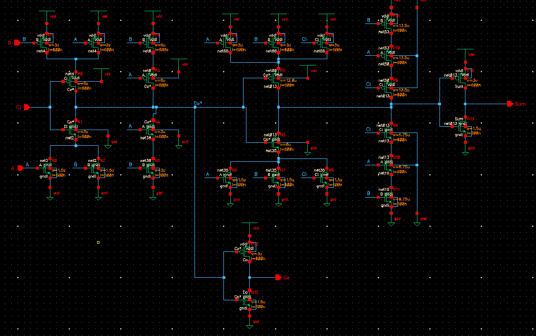
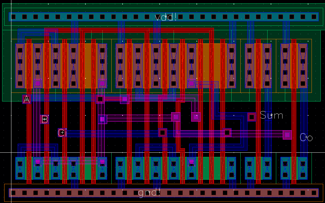
How much do I currently have? Well, I made a full adder. Not very impressive so far, but using TX gates instead of CMOS logic is something very interesting and I'm probably going to talk about in another day just because of how cool it is to me, coming from a fully-CMOS background.
Here are my schematic and layout for an adder:
At my school, I have Virtuoso for academia and I've gone through all the Cadence tutorials found at cmosedu. When I've followed the University of Nevada's EE 421/ECG 621 course, I noticed that the class is pretty much completed after these tutorials. The next step after that was their course project, which I haven't completed any of those, since most of them are pretty analog-focused. I'm more interested in getting the digital design and getting some background in there, so I decided that after those six tutorials, I had enough experience to start my own project, being the RISC V processor. Who knows if this is a good idea or not. Who cares, I'm learning so it doesn't really matter.
Why would I use Virtuoso instead of Magic (FOSS) for my IC design? Well, I don't know what I'm doing and Virtuoso has a lot of very nice tools for me to use. Since it's currently available to me right now, I'll just use what I've got. The main thing I have trouble with is getting my LVS (layout-vs-schematic) to generate properly. I'm still too inexperienced in layout design to be able to generate layouts properly and understand what's going on. I have a whiteboard that I draw my designs, get frustrated at it and think I have a design. Once I think it works, I try it out in Cadence, and if my LVS succeeds, I know that my design was correct. Most of the time, my LVS fails. Since I still fail LVS, and Magic doesn't even have LVS, I'm not knowledgeable enough to use Magic. I also don't know which software to use to design schematics for Magic's layout, sooo there's that.
As an ending note, I was unmotivated to continue, so hopefully adding this will get me motivated.
I really like the idea of having only a single metal layer for the cells. When I look at die shots of old ICs, I'm able to trace only a single metal layer, so I'm trying to replicate such designs. Here's my attempt at making a 2-1 mux using only a single metal layer:
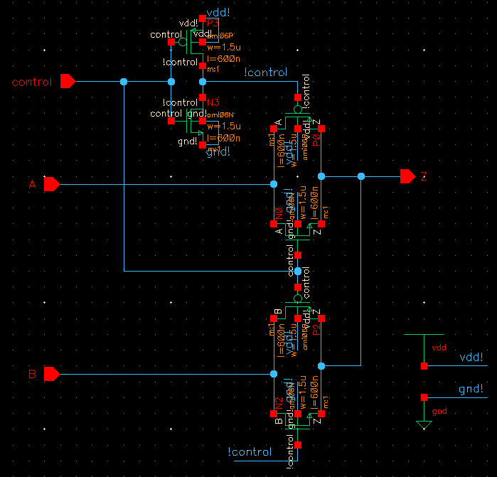
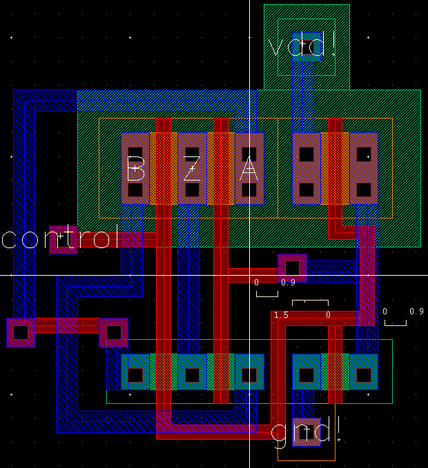
If you notice on the bottom left, I jumper A node from m1-to-poly-to-m1 (two jumps). I don't know if two jumps are okay for ICs, but I remember for PCBs, that you should try to only jump to one other layer before the connection. I assume this is the case from IC design, but I'll have to research more around.
Though, now that I'm thinking about it, whenever one uses a m1-m2 junction, one has to go from m1 to m2, then back to m1 again in order to reach the p- or n- active layer, so maybe two jumps is fine.
My research was pretty hectic this week, so I was only able to do around 3 hours of IC work this week! Bummer. I'll talk about TX gates later on, maybe make a new page all about it.
Next week, I'm going to research some memory architectures like SRAM. Maybe I'll be fancy and go for DRAM and then SDRAM. If I understand SDRAM enough, I'd love to design a full chip for that, since DDRx is of SDRAM type. I know that I can make some SRAM and DRAM cells, but designing the read/write buses will be interesting. My VLSI course back in the day had us design the schematic (not layout) of a SRAM cell, so I can cheat and go off of my knowledge from there. DRAM cells are super easy, but I think the control of them will be more difficult. I'm excited to learn about how to handle them; I have no idea.